HIGH SPEED DIGITAL, RF, POWER, MIXED SIGNAL, RF DESIGNS
Interfaces – DDR4, SFP, Ethernet, HDMI, USB
Controlled Impedance: Single Ended / Differential.
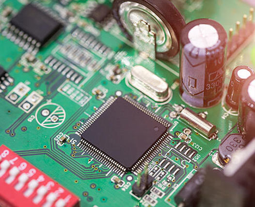
High Layer count (36 layers), High density designs.
Components more than 9000/BOARD, Connections more than 80000/BOARD
FP creation as per IPC7351 (A,B and C) including if any customer specifications standards.
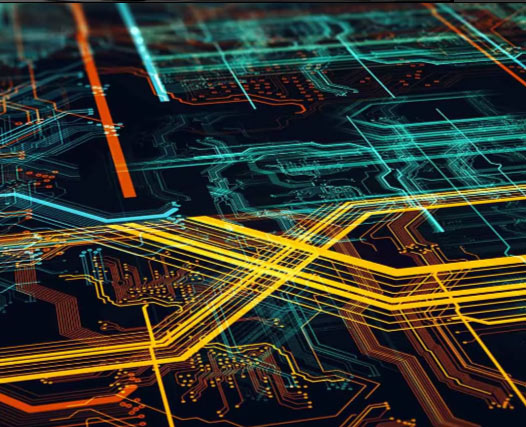
High speed interconnects: 10 Gbps.
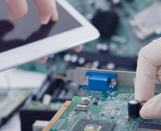
Critical and associated Components placement.
Fine pitch BGA upto 0.37mm, 2mil/2mil technology
Designs with Micro Vias, Blind Vias, Buried Vias and backdrill.
Stringent Thermal, Mechanical and Electrical requirements
Routing and Length matching of critical signals.
Generating Length reports of signals.
Gerber Setting and Fab, Assembly output Generation in 274X and ODB++ Format
Schematic Design
We can create symbols as per IEEE standards and will draw the schematics as per JEDEC standards.
Capturing Hand written schematic.
Integration of Schematic and Layout
Thermal Analasys
Board Level Thermal Design, simulation and analysis
PCB data import through IDF files available from all EDA tools.
Component Junction and case temperature computation.
Thermal profiles generation for components and PCB
SI Analasys
QDMS is experienced in cutting-edge technologies and access to latest tools; we can do SI / EMI analysis for the PCBs we design and third party designs.
Pre-route and post-route SI Analysis
Reflection Waveform Analysis and determination of termination scheme.
Reflection Waveform Analysis and determination of termination scheme.
Crosstalk analysis
Propagation delay and timing analysis
Eye Diagram Analysis
Multi-board analysis
Verification by extraction of actual PWB parasitic.
Placement optimization based on signal flow & trace length requirement of the specific interface.